







- About the Project
- STM32F4VE Hardware Overview
- Software & Toolchain
- Hardware Specifications
- PCB Stackup & Layer Configuration
- 3D Board Renders
- Schematic Design
- PCB Layout Views
- Design Verification
- How to Use
- Video Walkthrough
- Attribution
🏛️ FOSSEE Autumn Internship 2026 — Screening Task









This repository contains the complete printed circuit board design and schematic files for an STM32F4VE microcontroller development board. The design was developed as part of the screening task for the FOSSEE Autumn Internship program in 2026 at IIT Bombay.
The core of this board is the high-performance STM32F407VET6 IC, providing a robust hardware platform for advanced microelectronics and circuit design applications. The board features a black solder mask to replicate standard commercial STM development boards, with custom silkscreen graphics featuring the official FOSSEE logo, the STM logo, and the designer's name.
The STM32F4VE (STM32F407VET6) is a powerful, high-performance ARM Cortex-M4 core device widely used in embedded systems due to its balance of processing power, memory, and rich peripheral set.
|
|

STM32F407VET6 — Reference Development Board

Schematic Design |

PCB Layout |

3D Models / Symbols / Footprints |

Manufacturing Rules |
📌 Note: Schematic design was done in eSim 2.5, with PCB layout handled by KiCad 6 (integrated via eSim). All component libraries — 3D models, schematic symbols, and footprints — were sourced from SnapEDA.
🔧 Key Features at a Glance








|
|
The board is routed as a 4-layer PCB, specifically configured to comply with JLCPCB base model manufacturing rules.
| Layer | Name | Function |
|---|---|---|
| 🔴 Layer 1 | Front (F.Cu) | Signal routing and ground pour |
| 🟡 Layer 2 | Inner 1 (In1.Cu) | Dedicated ground plane |
| 🟢 Layer 3 | Inner 2 (In2.Cu) | Dedicated 3.3V power plane |
| 🔵 Layer 4 | Back (B.Cu) | Ground plane |
📐 Layer 1 — Front Copper
|
📐 Layer 2 — Inner Ground Plane
|
📐 Layer 3 — Inner Power Plane (3.3V)
|
📐 Layer 4 — Back Copper
|
🔍 Click to view individual PCB layer renders
|
Front Layer PCB
|
Back Layer PCB
|
|
Inner Layer 1 (In1.Cu)
|
Inner Layer 2 (In2.Cu)
|
All Layers Combined
|
All ICs Highlighted
|
🔝 Front View — 3D Render
|
🔽 Back View — 3D Render
|
📐 Side View — 3D Render
|
📐 Side Down View — 3D Render
|
🔍 Click to view additional 3D renders
3D Model Overview
|
Front — IC Close-up
|
Components Only View
|
PCB — Components Only (Alt)
|

Full Schematic Overview — eSim 2.5
🔍 Click to view schematic sections
Schematic — Section 1
|
Schematic — Section 2
|
📋 PCB — All Layers
|
📋 JLCPCB Gerber Preview
|
🔋 ERC — Electrical Rules Check
|
📏 DRC — Design Rules Check
|
✅ Electrical Rules Check (ERC): Passed with zero errors. Wire labels were utilized for power nets instead of standard power flags.
✅ Design Rules Check (DRC): Passed with zero errors, ensuring complete manufacturability compliance with JLCPCB specifications.
🔍 Click to view additional verification results
DRC — PCB View
|
Excluded ERC Warnings
|
1.  Download the project repository and extract the files.
2.  Open the schematic files using eSim 2.5 to view circuit connections.
3.  Open the PCB layout files in KiCad 6 to inspect:
      • Routing and trace widths
      • Layer stackup configuration
      • 3D model and component placement
4.  Generate Gerber files directly from KiCad for fabrication
    at any standard PCB manufacturer (JLCPCB recommended).
💡 Tip: All component libraries (3D models, symbols, footprints) are sourced from SnapEDA and should be imported into your KiCad library manager before editing.

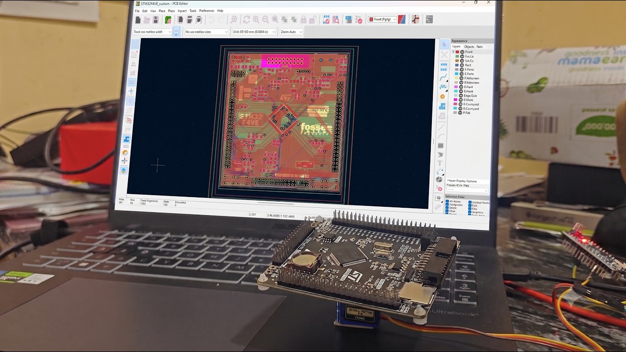
📹 Click to watch the complete project walkthrough on YouTube

Program Host |

PCB Design & Schematics |

Component Sources |


⭐ Star this repo if you found it useful! ⭐